
Stepping Up: How the Design of a Step Gold Finger PCB Differ from Traditional PCB Designs and Its Advantages
2024-06-05
In the world of printed circuit boards (PCBs), innovation never stops. As electronic devices become more complex and compact, the need for specialized PCB designs has grown. One such innovation is the Step Gold Finger PCB, a design that has gained popularity due to its unique structure and enhanced performance capabilities. This blog explores how the design of a Step Gold Finger PCB differs from traditional PCB designs and the advantages it offers.
Understanding Traditional PCB Design
Before diving into the specifics of Step Gold Finger PCBs, it's essential to understand the basics of traditional PCB designs. A standard PCB is a flat, multilayered board composed of various conductive and insulating layers. These layers are interconnected through vias (holes drilled through the board) and traces (thin lines of conductive material).
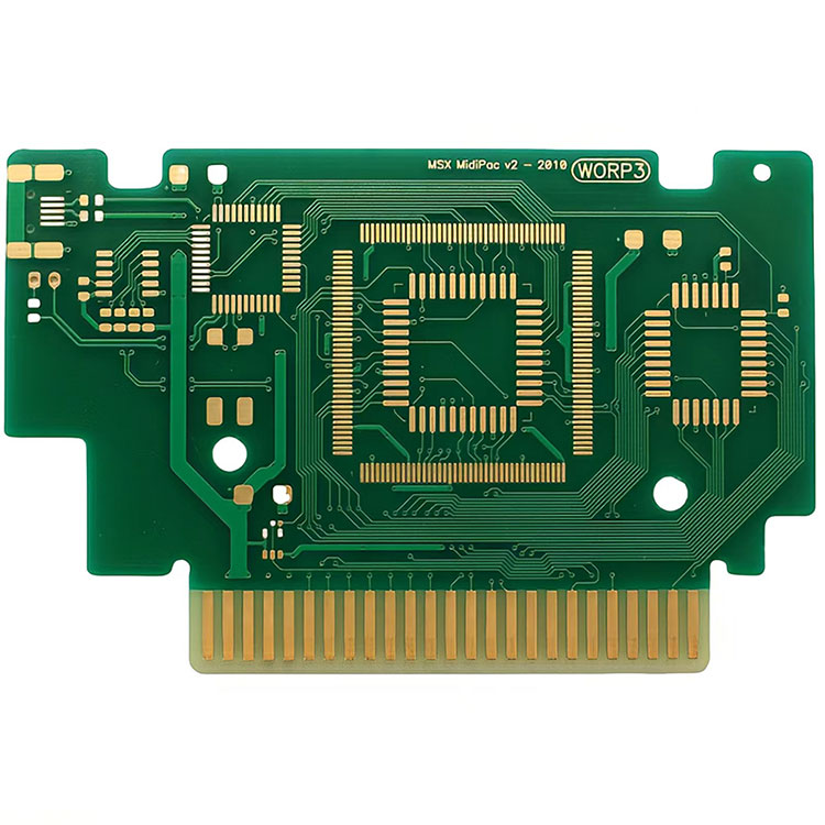
In traditional designs, gold fingers are used to create a reliable and robust connection between the PCB and other components or devices. These gold fingers are usually flat and positioned along the edges of the board, ensuring a stable electrical connection.
What is a Step Gold Finger PCB?
A Step Gold Finger PCB takes the concept of gold fingers a step further—literally. Unlike the traditional flat design, a Step Gold Finger PCB features a stepped or staggered configuration. This means that the gold fingers are placed at different heights or levels, creating a multi-tiered interface. This design is particularly useful in applications where multiple connections need to be made at different depths or where space constraints require a more compact and efficient connection method.
Key Differences in Design
1. Stepped Configuration: The most obvious difference is the stepped design of the gold fingers. Traditional PCBs have a uniform edge, while Step Gold Finger PCBs have varying levels, which can accommodate multiple connection points at different heights.
2. Increased Complexity: The manufacturing process for Step Gold Finger PCBs is more complex. It requires precise control over the plating process to ensure that each step is correctly coated with gold and that the thickness of the gold plating is uniform across all levels.
3. Customized Layout: The layout of a Step Gold Finger PCB is highly customized to fit specific applications. This often means that the design process involves more detailed planning and a higher degree of customization compared to traditional PCB designs.
Advantages of Step Gold Finger PCBs
1. Enhanced Connectivity: The stepped design allows for multiple connection points within a smaller area, which is ideal for complex devices requiring numerous connections. This increases the density of connections without compromising on reliability.
2. Space Efficiency: By using a multi-tiered approach, Step Gold Finger PCBs can significantly reduce the overall footprint of the board. This is especially beneficial in compact electronic devices where space is at a premium.
3. Improved Durability: The gold plating on the stepped fingers provides excellent resistance to corrosion and wear. This enhances the longevity and reliability of the connections, especially in environments where the PCB may be subject to frequent plugging and unplugging.
4. Versatility: The ability to customize the stepped configuration means that Step Gold Finger PCBs can be tailored to a wide range of applications, from consumer electronics to industrial machinery. This versatility makes them a valuable solution for various industries.
5. Better Signal Integrity: The precise control over the plating process and the layout of the stepped fingers can lead to improved signal integrity. This is crucial in high-frequency applications where signal loss and interference must be minimized.
Applications of Step Gold Finger PCBs
Step Gold Finger PCBs are used in various applications, including:
- Data Storage Devices: Enhancing connection density and reliability in hard drives and SSDs.
- Telecommunications: Ensuring robust connections in compact communication devices.
- Medical Equipment: Providing reliable and durable connections in critical medical devices.
- Automotive Industry: Supporting advanced electronics and compact designs in modern vehicles.
Conclusion
The Step Gold Finger PCB is a testament to the ongoing innovation in PCB design. By stepping up the traditional gold finger concept, this design offers enhanced connectivity, space efficiency, durability, versatility, and signal integrity. As electronic devices continue to evolve, the demand for such advanced PCB solutions will only grow, paving the way for even more sophisticated and reliable technologies.